

Microvia Failure Modes
A microvia is a small version of a through hole that is used in HDI printed circuit boards to form connections between layers. These small structures can be found on both bare and populated PCBs and can be filled or unfilled. While they offer advantages over traditional through holes, they are more susceptible to failure during the manufacturing process. This makes it important to understand the most common failure modes and how they can be avoided by following best practices.
Incomplete copper filling and voids in the plating of microvia increase stress levels within the structure and decrease microvia fatigue life. The size of the voids and the location in the via also have an impact on the microvia reliability. Large voids with a spherical shape increase the stress level while smaller voids with a cylindrical shape have lower impact.
As the demand for high-density interconnect (HDI) products continues to grow, so too does the need to avoid defects that cause these vias to fail during the production process. One of the most significant defects associated with HDI is called “plate-through-via separation,” a phenomenon that has become a major concern for electronics manufacturers and their customers. This type of defect causes the via to open up and close at different temperatures, which can lead to shorts and other electrical failures in the final product.
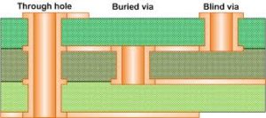
Microvia Failure Modes and How They Can Be Avoided
One of the most common reasons for plate-through-via separation is because the metals in the via experience different expansion rates during the reflow process. The differences between the coefficients of thermal expansion (CTE) of copper and dielectric material can cause a gap to form at the via interface, which is most often seen in the area of the cap plating. As the board undergoes repeated thermal excursions, the gap will widen over time, eventually causing the copper to separate from the underlying dielectric and the via to open up.
Another common issue is the tendency for the neck region of the microvia to fracture under extreme conditions such as high-aspect ratios and strong vibration or mechanical shock. This is due to the fact that copper curves inward near the via barrel and stress tends to concentrate there.
The good news is that microvias can be made more reliable through appropriate design practices, fabrication adherence to IPC-T-50M standards, and stackup configurations. Staggered microvias are also preferable over stacked ones as they have been shown to perform better during thermal shock testing. Additionally, continuous resistance monitoring during reflow and during thermal shock, with a 5% threshold at which the net fails, can be used to detect latent microvia failures that may otherwise go undetected.
To prevent these defects, Gauss Stack offers a computational prototyping service for microvias that includes a detailed thermomechanical simulation of your entire module or sub-assembly, subjected to your specified thermal conditions. This allows you to quickly identify if your microvias will survive the manufacturing process and the intended product life cycle. Contact us to learn more about how this can help you get your projects to market faster.