

Circuit Boards Manufactured
The demand for more complex and more capable electronic devices has created a need for the circuit board. Printed circuit boards are the insulating substrates that support component placement and make connections between the components.
A circuit board is made up of a dielectric composite material that contains an epoxy resin with woven or non-woven glass fibers and fillers. The composite materials are surrounded by copper foil. The dielectric layers are then encapsulated in an epoxy shell to keep out moisture and contaminants.
To produce a PCB, engineers start with blueprints or a computer-aided design (CAD) file. The CAD software is used to translate the schematic diagram into a layout of the inner and outer layers of the circuit board. The layout is then converted into a photomask that is printed on a clear Mylar sheet, usually at two or four times the actual size of the circuit board. Rub-on dry transfers of common component pin pads and traces increase efficiency.
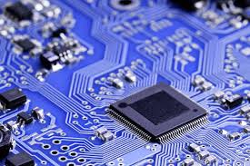
How Are Circuit Boards Manufactured?
After the photomask is printed, it is scanned and transformed into a digital image that will be used to print the PCB. The PCB is positioned under a machine that prints the image onto the surface of the circuit board. This process uses a special printer known as a plotter, which also makes the PCBs solder mask and silkscreen layers. The fabricator will use a computer to control the printing and to match the digital image with a pre-loaded CAD program that matches specifications for the desired print.
Depending on the design, the PCB may require either additive or subtractive manufacturing. Subtractive is the more common method, but it can be costly for complex designs. Additive, on the other hand, allows the use of a thicker layer of copper and lower cost for high-density layouts.
Once the circuit board is printed, holes are drilled in all of the exposed areas on the panel. These holes are used to connect the copper traces to the components, but they must be positioned carefully to ensure that the circuit board is properly oriented and routed. This requires that the traces be routed at specific widths to control impedance and prevent cross-talk between different signals.
When the traces are routed, they must be cleaned to remove any debris that may cause problems during assembly. A coating is applied to protect the copper from oxidation, and then the metal contact fingers are added. During this stage, the PCB is inspected for any defects. AOI (automated optical inspection) machines look for defects such as short circuits, excess copper and unmet specifications.
The next step is to solder the components. Once the components are placed and the connections are made, the conductive copper is plated with tin to make them more durable. The tin coating also helps the solder adhere to the copper, ensuring that the connections are solid. After the tin has been applied, the traces are polished to smooth out any rough spots. Then the boards are inspected again for any issues that could impact function, such as excessive copper, poor shape, or unmatched thickness. If the boards are good, they are packaged for distribution.