

Via in Pad
As PCB density increases and packages shrink, the design of vias becomes more challenging. Traditional vias use a connecting trace to transfer signals from the component pads to the board. This can result in routing issues such as annular rings, and size limitations when working with fine pitch IC packages like Quad Flat No Leads (QFN) or Ball Grid Arrays (BGA). Capped vias offer a solution to these problems and help to improve signal quality by eliminating the extra connection segment.
When a designer implements a capped via in a pad they are essentially putting an electrically non-conductive epoxy fill directly underneath the contact pads of the component. Once cured and planarized they are then plated over with copper to make the via a part of the component pad. This process is sometimes called “via tenting,” and it is necessary to prevent outgassing of the trapped air during soldering. The epoxy used for the fill also adds to the overall manufacturing cost of the PCB, and is one of the reasons why this design technique is more expensive than other forms of vias.
Another disadvantage of capped vias is that they increase the surface area of the pad and can lead to higher parasitic inductance. This is because the extra connection segment introduces a series resistance which can be a significant factor in signal integrity. To minimize this problem, it is important to optimize your PCB layout to minimize the amount of signal routing through this type of via.
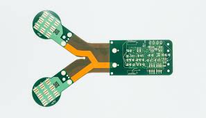
What is a Via in Pad?
The benefits of a via in pad are many and can have a big impact on the design of your circuit board. These advantages include the ability to use a smaller PCB footprint with increased density and using finer pitch components, as well as better heat transfer and reduced inductance.
Capped vias also help to simplify the layout of your PCB by allowing designers to route signal paths straight from the pad instead of through an extra connection segment. This allows bypass capacitors to be placed closer to the component, which can help lower parasitic inductance and EMF emissions.
To ensure that a designer only uses capped vias in the pads of their component, an additional manufacturing file is needed to be created with the proper drill data. This file should contain only the pads that will be capped and filled, while retaining the existing drill data for all other pads. Creating this file is easy with most PCB design tools and can help reduce confusion, as well as the costs associated with incorrectly specifying this technology.
Whether or not you decide to use via in pad for your next PCB project, it is essential to consult with your manufacturer to learn what their fabrication processes can handle. This will allow them to properly implement the technique and ensure that you don’t end up with a poorly fabricated PCB. Having this knowledge will allow you to take advantage of all the benefits that these vias can provide without sacrificing the performance of your finished product.