

PCB Printed Circuit Boards Are Used in Medical Devices
Medical devices come in a wide range of sizes and purposes, from small wearables that promote wellness to large full-body imaging systems. Whether they are designed to detect heartbeats, measure blood pressure, diagnose an illness, or simply provide comfort, they all depend on a pcb printed circuit board to function properly. These are the essential components that help healthcare professionals make accurate and timely decisions that can save lives.
As a result, the PCBs used in medical equipment must meet rigorous standards. They must uphold strict requirements regarding power, crosstalk, grounding, signal integrity, and other elements. They must also adhere to Class 3 electronic specifications for invasive medical devices and equipment. To ensure compliance with these industry-specific rules, partnering with a PCB manufacturing company that is experienced in producing Class 3 electronics is vital.
In addition to these specific rules, manufacturers must also consider the environmental conditions where their equipment will be used. The circuit boards will be subjected to a wide variety of temperatures, liquids, and shocks, so it’s important that they are able to withstand these extreme conditions. For example, the insulating material on medical-grade pcb printed circuit board should be resistant to chemicals and corrosion. It should also have a low coefficient of thermal expansion and high conductivity. This will help to minimize dimensional changes as the temperature of the circuit board changes.
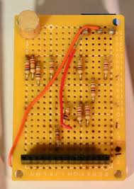
How PCB Printed Circuit Boards Are Used in Medical Devices
Medical-grade pcbs can also benefit from the use of special materials like polyimide, Teflon, and ceramic. These materials offer a lower dielectric constant than FR-4, which can help to reduce signal loss. They can also support higher-frequency performance and facilitate the implementation of high-density tracing. Finally, they can withstand harsh conditions, such as vibrations and continuous motion.
Due to the unique demands of medical-grade devices, a specialized PCB fabrication process is required. HDI technology is ideal for medical-grade PCBs, as it allows manufacturers to produce smaller, more dense designs with tighter tolerances on trace width and spacing. The technology also utilizes via-in-pad technology, which creates holes directly on the component pads, reducing the number of connections needed.
One of the primary advantages of PCBs lies in their reliability and consistency. Unlike traditional point-to-point wiring, where individual components are soldered together, PCBs provide a standardized platform for assembling and interconnecting components. This not only reduces the likelihood of human error during assembly but also minimizes the risk of electrical shorts and other malfunctions. Furthermore, PCBs facilitate mass production through automated assembly processes, making them cost-effective solutions for large-scale manufacturing.
SMT (Surface Mount Technology) is another popular assembly process for medical-grade PCBs. This technology removes the need for traditional soldering leads, which can improve reliability in a device that is exposed to vibrations and constant motion. Additionally, SMT components are smaller and can increase the overall component density on the PCB. This means that a larger number of components can fit on the same board, making it easier to meet IPC Class 3 requirements.